Photolithography is important part of any working nano-fabrication center. Photolithography produces a lateral pattern on a top of soft or solid materials. The exposed parts can be removed by etching. The technology can be applied several times creating complicated patterns and structures. The technology is used to produce patterns with resolution of 0.5 microns. Electron beam lithography (often abbreviated as e-beam lithography) is the practice of scanning a beam of electrons in a patterned fashion across a surface covered with a film of resist, "exposing" the resist, and of selectively removing either exposed or non-exposed regions of the resist under developing procedure. The primary advantage of electron beam lithography is that it is one of the ways to beat the diffraction limit of light and make features in the nanometer regime. This form of maskless lithography has found wide usage in photomask-making used in photolithography, low-volume production of semiconductor components, and research & development.
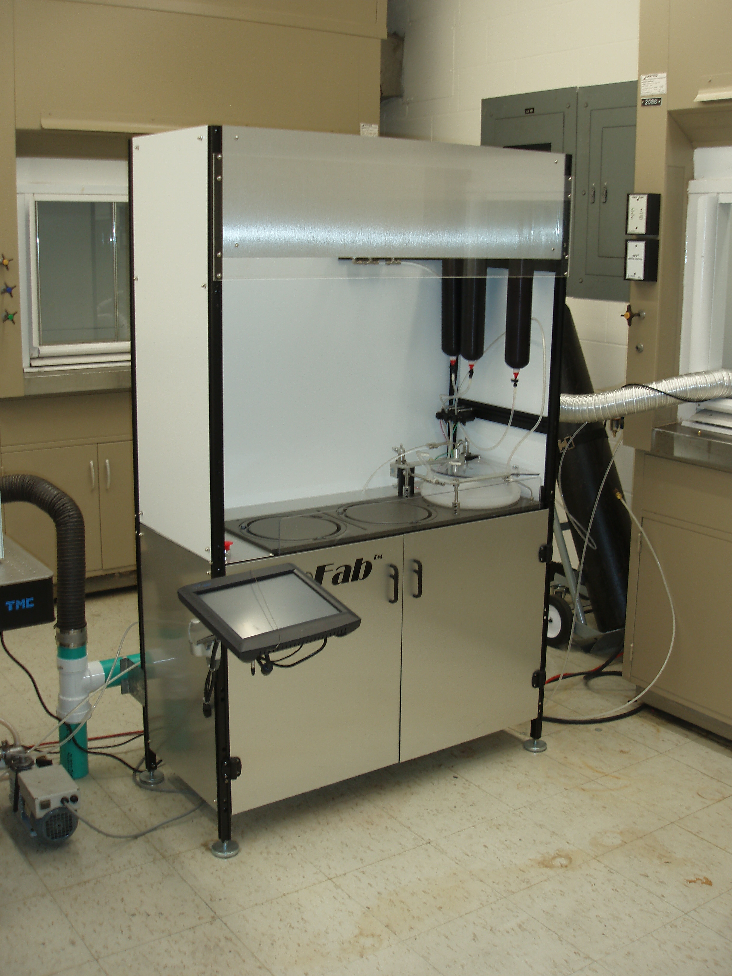
FOTOFAB PROCESS SYSTEM
The FotoFab process system provides precision spin coating suitable for Research and Development applications. The system includes the spinner and thermal modules with manual load option that requires the operator to load a holder and carry the wafer through the all process steps. The system is PC based with extensive process storage capabilities, programmable hot and cold plate temperatures, and programmable bake time. Reliable pneumatic actuators are used to move arms of programmable dispensers, centering device, and process chamber cover. Brushless DC drive spin motor provides speed up to 6000 rpm and acceleration up to 6000 rpm per second.
Staff:
Dr. Alexey Bykov
(212)650-5548
[email protected]
Location: CDI, 1.216
Hours: Contact Dr. Bykov to check process availability
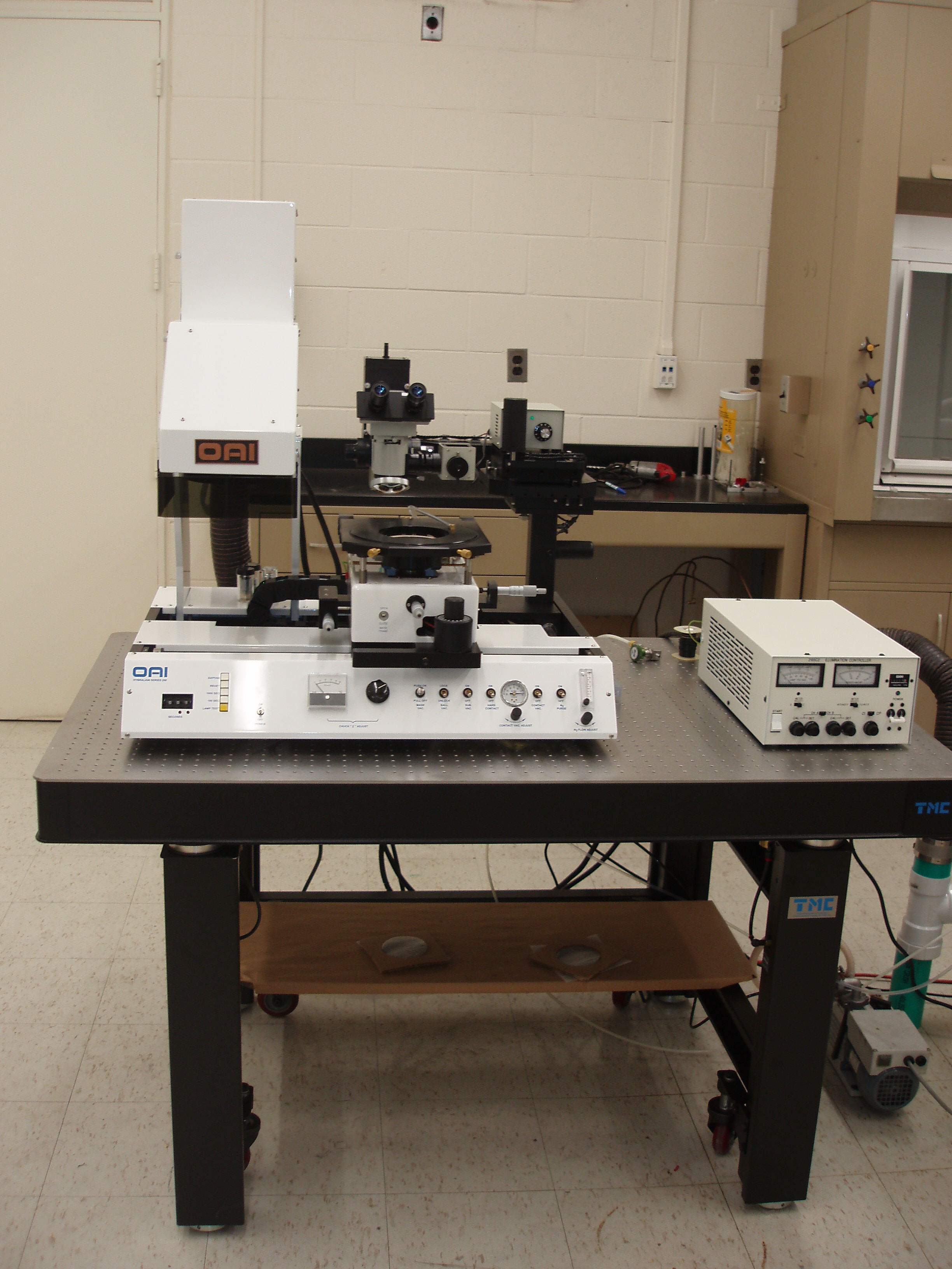
OAI HYBRALIGN 200 MASK ALIGNER
This system utilizes contact lithography to transfer photomask patterns onto substrates with manual wafer loading. Exposure methods: non-contact, soft contact, and soft-through-hard vacuum contact. High efficiency, extremely uniform, light source system consists on 350W lamphouse with UV400 optics (for 365 and 405nm exposures). Microscope with light power supply illumination controller provides numerous alignment options. Zero alignment shift when moving to expose position. 3" vacuum chuck and 4" maskholder (other size chuck and maskholder available by special order) provide processing wafers from 5mm up to 6".
Staff:
Dr. Alexey Bykov
(212)650-5548
[email protected]
Location: CDI, 1.222
Hours: Contact Dr. Bykov to check process availability
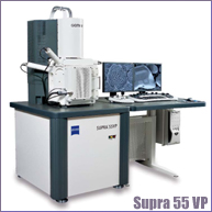
Electron beam lithography system (NPGS-Nabity) has been installed at SEM Supra 55VP
Staff:
Dr. Alexey Bykov
(212)650-5548
[email protected]
Location: MR022
Hours: Contact Dr. Bykov to check process availability
Wet chemistry area: fume hood, nitrogen jets, DI water
Staff:
Dr. Alexey Bykov
(212)650-5548
[email protected]
Location: CDI, 1.216
Hours: Contact Dr. Bykov to check process availability
Last Updated: 04/01/2024 10:47