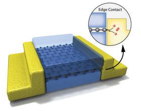
Illustration depicting atomically thin two-dimensional material, such as graphene, sandwiched between boron nitrite crystals, with electrical contact made along the material's one-dimensional edge.
As postdoc at Columbia, CCNY physicist Cory Dean and colleagues devised new method that addresses graphene’s contamination problem
Dr. Cory Dean, assistant professor of physics at The City College of New York, is the lead author of a paper published November 1 in the journal “Science” that demonstrates it is possible for an atomically thin two-dimensional (2D) material to have electrical contact along its one-dimensional (1D) edge. The contact architecture offers a new assembly technique for layered materials that prevents contamination at interfaces.
Professor Dean conducted the research as a postdoctoral fellow at Columbia University, working with Professor of Electrical Engineering Ken Shepard and Professor of Mechanical Engineering James Hone, the paper’s co-authors. The new method, which was developed using graphene as the two-dimensional model, resulted in the cleanest graphene produced to date.
“Two-dimensional materials such as graphene, which are just one atom thick, can have their electrical properties externally modified,” Professor Dean said. “However, because the materials are extremely sensitive to the environment, any external contamination quickly degrades performance.”
The need to protect the material from contamination while still allowing electrical access has been a roadblock to development of graphene-based technologies, he added. “By making contact only to the 1D edge of graphene, we have developed a fundamentally new way to bridge our 3D world to this fascinating 2D world without disturbing its inherent properties. This virtually eliminates external contamination and finally allows graphene to show its true potential in electronic devices.”
“Our novel edge-contact geometry provides more efficient contact than the conventional geometry without the need for further complex processing,” added Professor Shepard. “There are now many more possibilities in the pursuit of both device applications and the pure physics of clean systems.”
The researchers fully encapsulated the 2D graphene layer in a sandwich of thin insulating boron nitride crystals. To do this, they employed a new technique in which the top boron nitride crystal was used to sequentially pick up the other layers in the stack. “This technique completely eliminated any contamination between layers,” Professor Dean noted.
Once they created the stack, they etched it to expose the edge of the graphene layer. Then they evaporated metal onto the edge to create the electrical contact. By making contact along the edge, the team realized a 1D interface between the 2D active layer and 3D metal electrode.
Even though electrons entered only at the 1D atomic edge of the graphene sheet, the contact resistance was remarkably low, reaching 100 ohms per micron of contact width—a value smaller than what is typically achieved for contacts at the graphene top surface.
Continuing their collaboration, the team is now working on applying these techniques to develop new hybrid materials by mechanical assembly and edge contact. They plan to draw from the full suite of available 2D layered materials, including graphene, boron nitride, transition metal dichalcogenides (TMDCs), transition metal oxides (TMOs), and topological insulators (TIs).
“With so much current research focused on developing new devices by integrating layered 2D systems, potential applications are incredible, from vertically structured transistors, tunneling based devices and sensors, photoactive hybrid materials, to flexible and transparent electronics,” added Professor Hone.
On the Internet
About The City College of New York
Since 1847, The City College of New York has provided low-cost, high-quality education for New Yorkers in a wide variety of disciplines. More than 16,000 students pursue undergraduate and graduate degrees in: the College of Liberal Arts and Sciences; the Bernard and Anne Spitzer School of Architecture; the School of Education; the Grove School of Engineering; the Sophie Davis School of Biomedical Education, and the Colin L. Powell School for Civic and Global Leadership.
Set on a striking, 35-acre hilltop campus in upper Manhattan, CCNY has produced more Nobel laureates than any other public institution in the United States. The College has been touted as one of America's Top Colleges by Forbes, one of the Best Colleges in the United States as well as one of the Best Value Colleges by the Princeton Review, and ranks among U.S. News’ top regional universities.
MEDIA CONTACT
Ellis Simon
p: 212.650.6460
e:
[email protected]